Sunday, 29 July 2018

ALBERT EINSTEIN's Time Dilation - E = mc2 Explained

TIME AND THE MOVING CLOCK :

Time never seems to do what we want it to. There never seems to be enough of it when we're late for work or school, but far too much of it when we have to stand in the pouring rain waiting for a bus. These annoyances apart, it seems that time flows along smoothly; never bending, never changing its rate: always "on time". This steady flow is so reliable that we fit our lives around it. We start the day when the clock tells us to, work when it tells us to, eat when it tells us to, and go to bed when it tells us to. Time, it seems, is constant.


That the flow of time is constant is seemingly obvious and this has been the prevailing view for almost all of human history. Sir Isaac Newton, when he wasn't dodging falling apples, certainly thought time was constant. He gave us the idea of a "clockwork universe", in which it would be possible to know not only all of the past but all of the future if only we could say where every particle was, in what direction each particle was moving and at what speed. This model assumed, not unreasonably, that time flows at an ever constant rate. As brilliant as Newton was, he was, much to everyone's surprise, wrong.
                                                                 
In 1905 Albert Einstein published his Special Theory of Relativity. This work considered time not as a single constantly flowing entity, but as part of a much more complex system, linked with that of space itself. This is called space-time. Because space and time are part of the same entity it's impossible to move in space without moving in time. Time, for anything moving, changes.

One of the most startling consequences of special relativity is that any moving clock slows down relative to a stationary observer. There are of course many different types of clock, such as digital watches, clockwork clocks, atomic clocks and even our own biological clocks but they are all equally affected by the same principle, namely: MOVING CLOCK RUN SLOW.

Spacetime Diagrams :

The spacetime diagram is a useful visualisation technique.
The time axis is vertical, and of course we have multiplied t by c so we are measuring time in meters, the same as the other coordinates.
An object that is stationary does not have its position change with time: on a spacetime diagram this would be represented by a worldline that is vertical.
If an object is moving, its worldline is not vertical.
For something moving at the speed of light, it moves a distance of, say, 1 meter in a time of 1 meter. Thus the worldline makes an angle of 45 degrees with both the x and ct axes. In the diagram, we have drawn the light cone, representing rays of light that go through the point x=0 and ct=0.
The point x=0 and ct=0 is called the present. Coordinates in spacetime that are inside the light cone and have time coordinates greater than zero are in the future; locations inside the light cone with negative time are in the past.
                                                                       

Consider that we are located at the present. We know that, for example, we can not know what happened at the star Alpha Centauri yesterday; it is about 4 light years away and since no information can travel faster than the speed of light we will have to wait four years to find out what happened there. Thus the coordinate of Alpha Centauri yesterday, which is outside the light cone, is inaccessible to us. Similarly, we can not get a signal to Alpha Centauri that will arrive tomorrow. Thus the entire region of spacetime outside the light cone is called elsewhere.


WHY TIME RUN SLOW IN SPEED :

A reasonable question at this point is: if moving clocks run slowly,


We are going far too slowly for any noticeable change to take place.Even if we go at high enough speeds to bring about a large slowing down of local time we wouldn't notice because our own body clocks would also be running just as slowly.


The speed of light is very close to 300,000 km per second (186,300 miles per second). It isn't until we get to speeds that are a large fraction of the speed of light that any change in the flow of time becomes apparent. However, at speeds very close to that of light the effect grows in magnitude very rapidly indeed until time almost comes to a standstill.This slowing down of clocks due to high speeds is called time dilation and has a precise mathematical relationship. For the sake of completeness I have included the relevant equation below but you can skip over it and move on to the graph below it if you prefer. The equation for time dilation is:

When the equation is plotted as a graph we can easily see the dramatic effect of time dilation as the speed of light is approached:

So, when we move, at whatever speed, time slows down relative to a stationary observer. But note that, for example, the occupants of a rocket travelling at very high speeds would still experience time passing normally. However, if they could see out to an Earth-bound clock it would appear, to them, to be running too quickly. If an Earth-bound observer could see a clock inside the rocket it would appear to be running too slowly. This is why the theory is called "relativity", it is because time is relative to whoever is observing it at a particular speed.

MASS INCREASED DUE TO VELOCITY :

As our speed goes ever higher so the apparent mass increases, and so does the energy required to move it. At the speed of light it would take infinite energy to move any mass. Since it's clearly impossible to obtain infinite energy we can never quite reach the speed of light (but we can get as close as our energy supply, and technology, will allow). Note that the occupants of any rocket travelling at very high speeds will not be aware of any increase in mass, just as they wouldn't be aware in any change in the rate that time passes. It's only when they measure the mass of stationary observers that they will see that there has been a change in mass -- the astronauts will perceive that everything around them and their rocket has changed its mass while their own seems to have remained constant


Relativistic Mass Formula
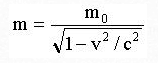
Relativistic mass refers to mass of a body which change with the speed of the body as this speeds approaches close to speed of light, it increases with velocity and tends to infinity when the velocity approaches the speed of light.
Relativistic mass = rest mass / squared root [one minus (velocity / speed of light) squared]
The equation is:
mr = m0 / sqrt (1 – v2 / c2 )
Where:
mr: relativistic mass
m0: rest mass (invariant mass)
v: velocity
c: speed of light

THE EQUATION  :
In order to compensate for the apparent mass increase due to very high speeds we have to build it into our equations. We know that the mass increase can be accounted for by using the equation:

From this equation we know that mass (m) and the speed of light (c) are related in some way. What happens if we set the speed (v) to be very low? Einstein realized that if this is done we can account for the mass increase by using the term mc2 (the exact arguments and mathematics required to derive this are quite advanced, but an example is provided here). Using this term we now have an equation that takes into account both the kinetic energy and the mass increase due to motion, at least for low speeds


This equation seems to solve the problem. We can now predict the energy of a moving body and take into account the mass increase. What's more, we can rearrange the equation to show that:
This result is fine for low speeds, but what about speeds closer to the speed of light? We know that mass increases at high speeds, but according to the Newtonian part of the equation that isn't the case. Therefore, we need to replace the Newtonian part of the formula in order to make the equation correct at all speeds. How can we do this?We know that E – mc2 is approximately equal to the Newtonian kinetic energy when v is small, so we can use E – mc2 as the definition of relativistic kinetic energy:
We have now removed the Newtonian part of the equation. Note that we haven’t given a formula for relativistic kinetic energy. The reason for this will become apparent in a moment. Rearranging the result shows that:
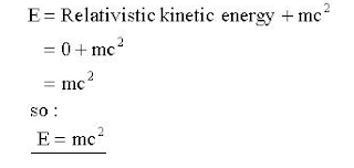
It can now be seen that relativistic energy consists of two parts. The first part is kinetic and depends on the speed of the moving body, while the second part is due to the mass increase and does not depend on the speed of the body. However, both parts must be a form of energy, but what form? We can simplify the equation by setting the speed (i.e. the relativistic kinetic energy) of the moving body to be zero, thereby removing it from the equation:
We now have the famous equation in the form it's most often seen in, but what does it mean?We have seen that a moving body apparently increases in mass and has energy by virtue of its speed (the kinetic energy). Looking at the problem another way we can say that as the speed of a body gets lower there will be less and less kinetic energy until at rest the body will have no kinetic energy at all. So far so good, but what about the mass due to the speed of the body? Again, as the body slows down the mass will become progressively smaller but it can't reach zero. As noted near the start of the page, the lowest the mass can be is unity (1) and we can't just make the body disappear into nothing. The lowest possible mass the body can have is its "rest mass", i.e. the mass the body has when it is at rest. But the equation we have derived (E = mc2) isn't for mass, it's for energy. The energy must somehow be locked up in the mass of the body

:


Saturday, 28 July 2018

WORKING OF TRANSISTORS

How Transistors Work – A Simple Explanation :

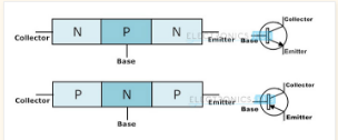
Transistors are composed of three parts a base, a collector, and an emitter. The base is the gate controller device for the larger electrical supply. The collector is the larger electrical supply, and the emitter is the outlet for that supply. By sending varying levels of current from the base, the amount of current flowing through the gate from the collector may be regulated. In this way, a very small amount of current may be used to control a large amount of current, as in an amplifier.

 The same process is used to create the binary code for the digital processors but in this case a voltage threshold of five volts is needed to open the collector gate. In this way, the transistor is being used as a switch with a binary function: five volts  ON, less than five volts OFF. 


quantum mechanical transistor  :

The quantum mechanical transistor is the equivalent of turning on a light bulb without closing a switch: Electrons "tunnel" from path to path through a barrier that, according to classical physics, is impenetrable.
The process takes place with extreme rapidity.
The term "tunneling" may bring to mind moles or the highway department, but physicists use it to describe an effect in which particles, like electrons, appear in places where by rights they should not be able to go. In effect, they have tunneled under an energy barrier the same way cars use a tunnel to appear at a new location without having to drive over an impossibly high summit. The atomic-scale effect is explained only by quantum mechanical principles.

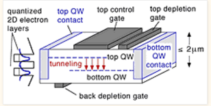
The device, dubbed DELTT (Double Electron Layer Tunneling Transistor), offers promise of significant improvements in the speed of computers and in the accuracy of sensors. 

The very fast device may run at a trillion operations a second, as have other, more primitive tunneling devices. This is roughly ten times the speed of the fastest transistor circuits currently in use. Actual speed has not yet been measured
 **The extremely fast device also runs at extremely low power tens of millivolts and microamps  as compared with the few volts and milliamps needed by transistors currently in use.

How it works :

The technique relies in part upon the dual wave-particle nature of matter. In the device, two gallium arsenide layers, each only 150 angstroms thick, are separated by a 125 angstrom aluminum-gallium- arsenide barrier , the equivalent of the yards of two houses separated by a sturdy fence. Ordinarily, gallium arsenide electrons in one yard do not have the energy to climb the fence to reach the other yard. But the tiny thickness of the barrier causes the electrons to behave like waves, which can poke into the barrier.

When an electron is adjusted to have the same energy and momentum states in both regions -- something that can be done by applying a voltage to these regions -- it can pass from one region to the other without any scattering, as occurs in normal electron motion due to crystal imperfections. In effect, they tunnel under the barrier fence.

Types of transistor  :


There are two main types of transistors-junction transistors and field effect transistors.
 Each works in a different way. But the usefulness of any transistor comes from its ability to control a strong current with a weak voltage. For example, transistors in a public address system amplify (strengthen) the weak voltage produced when a person speaks into a microphone. The electricity coming from the transistors is strong enough to operate a loudspeaker, which produces sounds much louder than the person's voice. 

Bipolar junction transistor  ( BJT ) : 

A junction transistor consists of a thin piece of one type of semiconductor material between two thicker layers of the opposite type. For example, if the middle layer is p-type, the outside layers must be n-type. Such a transistor is an NPN transistor. One of the outside layers is called the emitter, and the other is known as the collector. The middle layer is the base. The places where the emitter joins the base and the base joins the collector are called junctions. 


The layers of an NPN transistor must have the proper voltage connected across them. The voltage of the base must be more positive than that of the emitter. The voltage of the collector, in turn, must be more positive than that of the base. The voltages are supplied by a battery or some other source of direct current. The emitter supplies electrons. The base pulls these electrons from the emitter because it has a more positive voltage than does the emitter. This movement of electrons creates a flow of electricity through the transistor. 


The current passes from the emitter to the collector through the base. Changes in the voltage connected to the base modify the flow of the current by changing the number of electrons in the base. In this way, small changes in the base voltage can cause large changes in the current flowing out of the collector.
there is 4 common types of biasing of transistor,
  1. BASE BIAS
  2. COMMON EMITTER BIAS
  3. COLLECTOR FEEDBACK BIAS
  4. VOLTAGE DEVIDER BIAS


FIELD EFFECT TRANSISTORS :


A field effect transistor has only two layers of semiconductor material, one on top of the other. Electricity flows through one of the layers, called the channel.

 A voltage connected to the other layer, called the gate, interferes with the current flowing in the channel. Thus, the voltage connected to the gate controls the strength of the current in the channel. There are two basic varieties of field effect transistors-the junction field effect transistor(JFET) 
and the metal oxide semiconductor field effect transistor (MOSFET).
 ***Most of the transistors contained in today's integrated circuits are MOSFETS's.


Applications of Transistors :


A . The transistor as an amplifier 


1. A transistor can be used to amplify current. This is because a small change in base current causes a large change in collector current.

2. Example is a microphone. 

3. Sound waves that are fed into the microphone cause the diaphragm in the microphone to vibrate. 

4. The electrical output of the microphone changes according to the sound waves. 

5. As a result, the base current is varying because of the small alternating voltage produced by the microphone. 

6. A small change in the base current causes a large change in the collector current. 

7. The varying collector current flows into the loudspeaker. There, it is changed into the sound waves corresponding to the original sound waves. 

8. The frequencies of both waves are equivalent but the amplitude of the sound wave from the loudspeaker is higher than the sound waves fed into the microphone. 

Component: Function

Microphone: To change sound signal to electrical signal 

Capacitor: To block a steady current from flowing into the transistor and microphone. 

Potential divider: To apply a proportion of the total voltage across the emitter-base junction so that 
the junction is forward-biased. 

Transistor: To amplify the input wave form. 

Loudspeaker: To change the electrical signal to sound wave. 


B. The transistor as switch 


1. In a transistor, no current can flow in the collector circuit unless a current flows in the base circuit. This property allows a transistor to be used as switch.

2. The transistor can be turned on or off by changing the base. 

3. There are a few types of switching circuits operated by transistors. 

C. Light-Operated Switch

1. The circuit is designed to light the bulb in a bright environment and to turn it off in the dark.

2. One of the components in the potential divider is a light-dependent resistor (LDR). When it is placed in DARKNESS, its resistance is large. The transistor is switched OFF. 

3. When LDR is lighted by bright light, its resistance falls to small value resulting in more supply voltage and raising the base current. The transistor is switched on, collector current flows and bulb lights up. 

D. Heat-operated switch

1. One important component in the circuit of a heat-operated switch is the thermistor.

2. Thermistor is type of resistor that responds to the surrounding temperature. Its resistance increases when the temperature is low and vice versa. 

3. When heat is applied to the thermistor, its resistance drops and a greater share of supply voltage is dropped across R. The base current increases followed by a greater increase in the collector current. The bulb will glow and the siren will sound. 

4. This particular circuit is suitable as a fire alarm system. 

E. Integrated Circuits 

1. An integrated circuit (IC) consists of transistors, resistors, diodes and capacitors combined together in one wafer-thin chip of silicon.

2. This is one wafer-thin chip is called a microchip. 

3. The microchip is only a few millimeters square with a thickness of 0.5 mm.

HOW ZENER DIODE WORKS

Zener Diode Working Function


Zener diodes are normal P-N junction diodes operating in a reverse biased condition. Working of the Zener diode is similar to a P-N junction diode in forward biased condition, but the uniqueness lies in the fact that it can also conduct when it is connected in reverse bias above its threshold / breakdown voltage.


 These are among the besic types of diodes used frequently, apart from the normal diodes.


Principle behind Zener diode Working :

As stated above the basic principle behind the working of a zener diode lies in the cause of breakdown for a diode in reverse biased condition. Normally there are two types of breakdown- Zener and Avalanche.
   

Zener Breakdown :

This type of breakdown occurs for a reverse bias voltage between 2 to 8V.  Even at this low voltage, the electric field intensity is strong enough to exert a force on the valence electrons of the atom such that they are separated from the nuclei. This results in formation of mobile electron hole pairs, increasing the flow of current across the device.  Approximate value of this field is about 2*10^7 V/m.
This type of break down occurs normally for highly doped diode with low breakdown voltage and larger electric field. As temperature increases, the valence electrons gain more energy to disrupt from the covalent bond and less amount of external voltage is required. Thus zener breakdown voltage decreases with temperature.
Avalanche breakdown
This type of breakdown occurs at the reverse bias voltage above 8V and higher.  It occurs for lightly doped diode with large breakdown voltage.  As minority charge carriers (electrons)flow across the device, they tend to collide with the electrons in the covalent bond and ,cause the covalent bond to disrupt.As voltage increases, the kinetic energy (velocity) of the electrons also increases and the covalent bonds are more easily disrupted, causing an increase in electron hole pairs. The avalanche breakdown voltage increases with temperature.So there is a relation between tempareture.

Zener diode applications :

Voltage regulator :


The load voltage equals breakdown voltage V-Z of the diode. The series resistor limits the current through the diode and drops the excess voltage when the diode is conducting.

Zener diode in overvoltage protection :

If the input voltage increases to a value higher than the Zener breakdown voltage, current flows through the diode and create a voltage drop across the resistor; 
this triggers the SCR and creates a short circuit to the ground. The short circuit opens up the fuse and disconnects the load from the supply.

Zener Diode Clipping Circuits :
Zener diodes are used to modify or shape AC waveform clipping circuits.

The clipping circuit limits or clips off parts of one or both of the half cycles of an AC waveform to shape the waveform or provide protection.


Zener Diode Reference
Here is a handy zener diode list if you work with these critters.  This list is far from complete, but these are some common numbers we encounter.


HOW A DIODE WORKS

Introduction to Diodes :


The Diode can be considered as the simplest and most fundamental element in electronics, which is composed of a p-n Junction. It is a two terminal device,

 shows its schematic symbol, where the "+" terminal is called Anode and is connected to the p-Region and the "-" terminal is called Cathode and is connected to the n-Region.


Symbol of Diode :

The symbol of a diode is shown below. The arrowhead points in the direction of conventional current flow.
We can create a simple P-N junction diode by doping donor impurity in one portion and accept impurity in other portion of silicon or germanium crystal block. These doping make a P-N junction at the middle part of the block beside which one portion becomes p-type (doped with trivalent or accept impurity), and another portion becomes n-type (doped with prevalent or donor impurity). We can also form a P-N junction by joining a p-type (doped with a trivalent impurity) and n-type ( doped with a prevalent impurity) together with a special fabrication technique. Hence, it is a device with two elements, the p-type forms anode, and the n-type forms the cathode.

Working Principle of Diode

Forward Biased Diode

In a P-N junction diode when the forward voltage is applied i.e. positive terminal of a source is connected to the p-type side, and the negative terminal of the source is connected to the n-type side, the diode is said to be in forward biased condition. We know that there is a barrier potential across the junction. This barrier potential is directed in the opposite of the forward applied voltage. So a diode can only allow current to flow in the forward direction when forward applied voltage is more than barrier potential of the junction. This voltage is called forward biased voltage. For silicon diode, it is 0.7 volts. For germanium diode, it is 0.3 volts. When forward applied voltage is more than this forward biased voltage, there will be forward current in the diode, and the diode will become short circuited.
Hence, there will be no more voltage drop across the diode beyond this forward biased voltage, and forward current is only limited by the external resistance connected in series with the diode. Thus, if forward applied voltage increases from zero, the diode will start conducting only after this voltage reaches just above the barrier potential or forward biased voltage of the junction. The time, taken by this input voltage to reach that value or in other words, the time, taken by this input voltage to overcome the forward biased voltage is called recovery time.

Reverse Biased Diode

Now if the diode is reverse biased i.e. positive terminal of the source is connected to the n-type end, and the negative terminal of the source is connected to the p-type end of the diode, there will be no current through the diode except reverse saturation current. This is because at the reverse biased condition the depilation layer of the junction becomes wider with increasing reverse biased voltage. Although there is a tiny current flowing from n-type end to p-type end in the diode due to minority carriers. This tiny current is called reverse saturation current. Minority carriers are mainly thermally generated free electrons and holes in p -type and n- type respectively. Now if reverse applied voltage across the diode is continually increased, then after certain applied voltage the depletion layer will destroy which will cause a huge reverse current to flow through the diode.

 If this current is not externally limited and it reaches beyond the safe value, the diode may be permanently destroyed. This is because, as the magnitude of the reverse voltage increases, the kinetic energy of the minority charge carriers also increase. These fast moving electrons collide with the other atoms in the device to knock-off some more free electrons from them. The free electrons so released further release much more free electrons from the atoms by breaking the covalent bonds. This process is termed as carrier multiplication and leads to a considerable increase in the flow of current through the p-n junction.


Quantum tunneling relation with diode : 

is the passing of electrons through an insulating barrier which is thin compared to the de-Broglie .electron wavelength. If the “electron wave” is large compared to the barrier, there is a possibility that the wave appears on both sides of the barrier.
In classical physics, an electron must have sufficient energy to surmount a barrier. Otherwise, it recoils from the barrier. (Figure) Quantum mechanics allows for a probability of the electron being on the other side of the barrier. If treated as a wave, the electron may look quite large compared to the thickness of the barrier. Even when treated as a wave, there is only a small probability that it will be found on the other side of a thick barrier. See green portion of curve, (Figure). Thinning the barrier increases the probability that the electron is found on the other side of the barrier.

Tunnel diode: 

The unqualified term tunnel diode refers to the esaki tunnel diode, an early quantum device. A reverse biased diode forms a depletion region, an insulating region, between the conductive anode and cathode. 
This depletion region is only thin as compared to the electron wavelength when heavily doped– 1000 times the doping of a rectifier diode. With proper biasing, quantum tunneling is possible. 

Types of Diode

The types of diode are as follow :

  1. Zener diode
  1. P-N junction diode
  1. Tunnel diode
  1. varactor diode
  1. Schottky diode
  1. Photo diode
  1. PIN diode
  1. LASER diode
  1. Avalanche diode
  1. Light emitting diode


WHAT IS ANTIMATTER

ANTI-MATTER : Antimatter is the opposite of normal matter. More specifically, the sub-atomic particles of antimatter have properties ...